
Discover how semiconductors work in this beginner guide. Learn about silicon wafers, transistors, and the tiny chips that power our iPhones and AI in 2026.
- The Basic Science of Conductors and Insulators
- Doping: Creating N Type and P Type Silicon
- The Transistor: The World’s Smallest Switch
- How Chips are Made: The Manufacturing Marathon
- The Global Supply Chain and Geopolitics
- Semiconductors and the AI Boom
- The Future: Beyond Silicon
- Key Takeaways for Beginners
- Conclusion
- Frequently Asked Questions
Everything you touch today likely relies on a tiny piece of silicon.
From the smart refrigerator in your kitchen to the advanced iPhone 17 AI features in your pocket, chips are the brain of the digital age.
Understanding how semiconductors work is no longer just for engineers. It is essential knowledge for anyone who wants to understand the global economy and the future of technology.
As we move further into 2026, these microscopic components have become the most valuable resource on the planet.
A semiconductor is a unique material that sits between a conductor and an insulator. This means it can sometimes allow electricity to flow and sometimes block it.
This simple ability to “switch” is what allows computers to process information using binary code. By controlling the flow of electrons, scientists can create complex logic that powers everything from basic calculators to advanced artificial intelligence.
This guide will break down the complex physics into simple steps that anyone can follow.
The Basic Science of Conductors and Insulators
To understand how semiconductors work, you first need to look at how electricity moves through materials.
Most materials fall into two categories. Conductors like copper or gold have “loose” electrons that move easily.
This makes them perfect for wires that carry power to your home. On the other hand, insulators like rubber or glass hold onto their electrons tightly.
This prevents electricity from flowing where it should not go.
Semiconductors are special because they are “moody.” Under some conditions, like high heat or the presence of a specific light, they act like conductors.
Under other conditions, they act like insulators. This dual nature is why they are called “semi” conductors. Silicon is the most common material used for this purpose.
It is found in abundance in sand, making it a cost effective choice for global manufacturing.
The Role of the Atomic Structure
The secret lies in the atoms of the silicon. Each silicon atom has four electrons in its outer shell. In a pure crystal of silicon, these atoms bond together perfectly.
This leaves no “free” electrons to move around. In its pure state, silicon is actually a fairly poor conductor.
It behaves more like an insulator because the electrons are locked in place.
To make silicon useful for electronics, scientists must “mess it up” on purpose. This process is called doping.
By adding a tiny amount of another element, researchers can change the electrical properties of the crystal. This is the fundamental step in the process of how semiconductors work.
Without doping, the silicon would just be a beautiful but useless piece of glass.

Doping: Creating N Type and P Type Silicon
There are two main ways to dope silicon. The first method involves adding an element like phosphorus. Phosphorus atoms have five electrons in their outer shell.
When a phosphorus atom replaces a silicon atom in the crystal, it has one extra electron left over.
This creates a “negative” charge carrier. Scientists call this N type silicon.
The second method involves adding an element like boron. Boron atoms only have three electrons in their outer shell.
When boron is added to the silicon, it creates a “hole” where an electron should be. You can think of this hole as a positive charge that can move around.
This creates P type silicon. By putting N type and P type silicon together, engineers can control electricity with incredible precision
The PN Junction and the Diode
When you join a piece of P type silicon to a piece of N type silicon, something magical happens at the border. This border is called a PN junction.
Electricity can flow in one direction across this border but not the other. This creates a device called a diode.
Diodes are used to turn alternating current from your wall outlet into the direct current that your laptop uses.
This one way street for electrons is the foundation for more complex parts. It is the simplest example of how semiconductors work in a real world circuit.
By stacking these junctions in different ways, engineers can create “gates” that open and close.
These gates are the building blocks of every digital device ever made.
The Transistor: The World’s Smallest Switch
The most important invention in the history of semiconductors is the transistor. You can think of a transistor as a tiny light switch that has no moving parts.
It uses a small electrical signal to control a much larger flow of electricity. This allows the chip to represent a “1” when the switch is on and a “0” when the switch is off.
Today, a single chip inside your phone contains billions of these transistors. They are so small that you could fit thousands of them across the width of a single human hair.
The evolution of the transistor is what allows the iPhone 17 AI features to process complex data so quickly.
As transistors get smaller, we can fit more of them on a chip, making our devices more powerful and more efficient every year.
How Binary Logic Powers AI
Because transistors can be either on or off, they speak the language of binary. Computers use strings of ones and zeros to represent everything from a text message to a high definition video.
In 2026, AI models use billions of these binary operations to “think.” When you ask your phone to recognize a face or translate a sentence, it is actually just flipping trillions of tiny transistor switches.
The speed at which these switches flip is measured in gigahertz. A three gigahertz processor can flip its transistors three billion times every second.
This incredible speed is why modern AI feels so intelligent. It is not that the computer is smart in a human way. It is just performing math at a scale that is hard for the human brain to imagine.

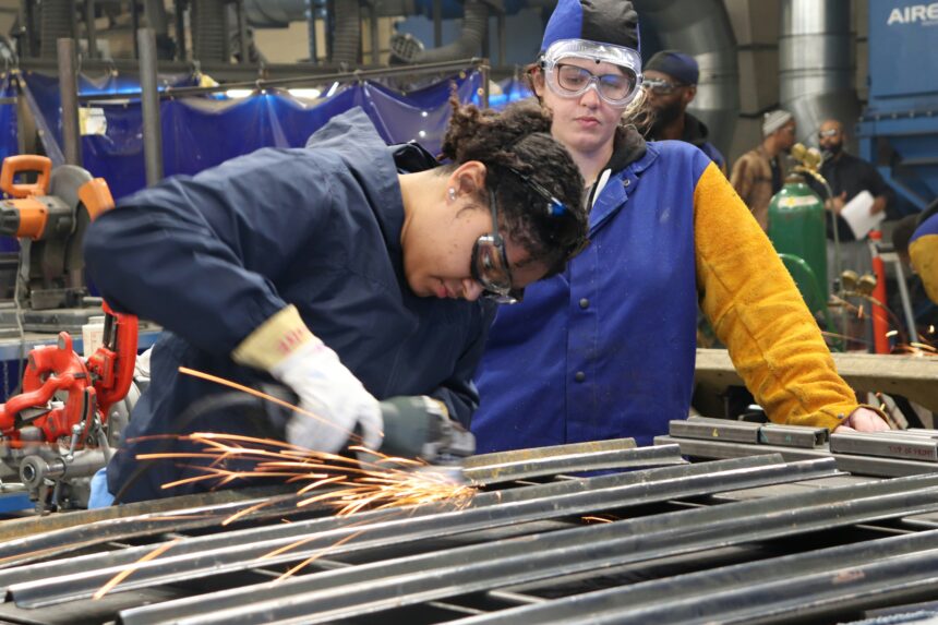
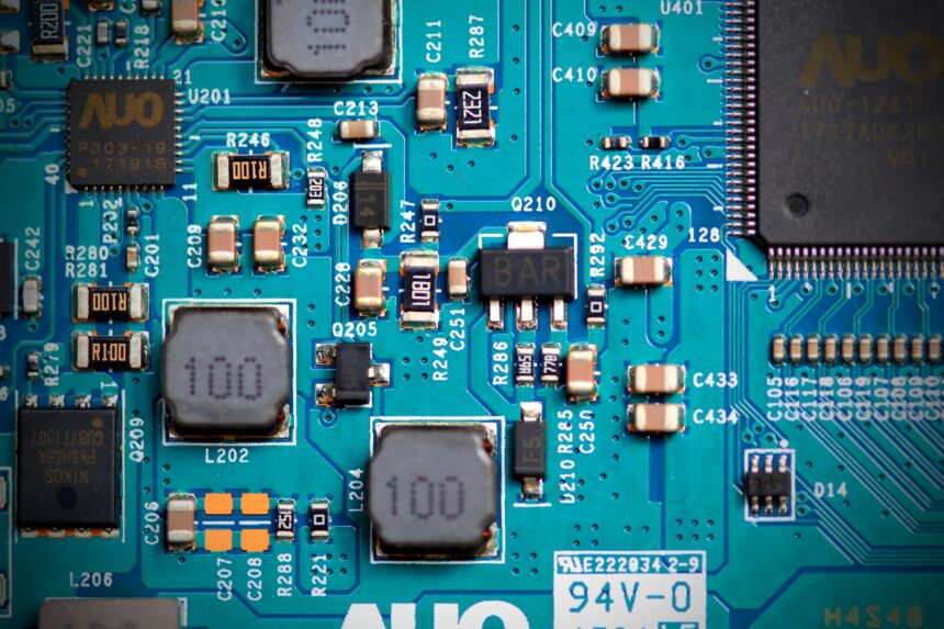
How Chips are Made: The Manufacturing Marathon
Making a semiconductor chip is the most complex manufacturing process in human history. It takes months to turn a raw piece of silicon into a finished processor.
The process begins with a “wafer,” which is a thin disc of pure silicon. This wafer is polished until it is perfectly flat and reflects light like a mirror.
The manufacturing takes place in “clean rooms.” These facilities are thousands of times cleaner than an operating room in a hospital. Even a single speck of dust can ruin a chip.
Workers must wear full body “bunny suits” to prevent hair or skin cells from falling onto the wafers. This level of precision is necessary because the features on the chip are measured in nanometers.
Photolithography and the 2nm Revolution
To get the designs onto the silicon, engineers use a process called photolithography. It is similar to how a traditional camera uses light to print a photo onto film.
A machine called a “stepper” shines ultraviolet light through a mask that contains the circuit pattern. This light hits a chemical coating on the wafer, “printing” the design into the silicon.
In 2026, the industry has moved toward two nanometer (2nm) technology. These machines, built largely by a company called ASML, use “Extreme Ultraviolet” light.
This light has a wavelength so short that it can carve features that are almost as small as individual atoms. This is the peak of how semiconductors work today.
The smaller the features, the less power the chip uses and the faster it runs.
The Global Supply Chain and Geopolitics
No single country can make a modern chip alone. The semiconductor supply chain is truly global. The designs often come from companies in the United States like Apple or Nvidia.
The machines used to print the chips come from the Netherlands. The chemicals and specialty gases often come from Japan. Finally, the actual manufacturing mostly happens in Taiwan and South Korea.
This interdependence makes the industry very sensitive to global events. If there is a trade dispute or a natural disaster in one part of the world, it can cause a shortage of chips everywhere.
This is why many governments are now spending billions of dollars to build their own “fabs” or chip factories. They want to ensure they always have access to the chips that power their military and economy.
The Dominance of TSMC
The Taiwan Semiconductor Manufacturing Company (TSMC) is currently the most important company in the world that you might not know.
They make the chips for almost everyone, including Apple and AMD. Because they have the most advanced technology, everyone competes for space in their factories.
When you hear about the latest iPhone 17 AI features, remember that those chips were likely born in a TSMC facility in Taiwan.
The complexity of these factories is staggering. A single modern fab can cost over 20 billion dollars to build.
This high cost of entry means only a few companies in the world can compete at the highest level. This “bottleneck” is why semiconductors are often called the “new oil” of the 21st century.

Semiconductors and the AI Boom
The rise of artificial intelligence has changed the types of chips we need. Traditional CPUs are like a few very smart professors who can solve any problem.
However, AI needs thousands of “elementary students” who can all do simple math at the same time. This is why GPUs, or Graphics Processing Units, have become so popular.
Companies like Nvidia have seen their value skyrocket because their chips are designed for this “parallel processing.” Instead of doing one task at a time, an AI chip does thousands.
This allows a computer to train on massive amounts of data in a short time. In 2026, we are seeing “NPU” or Neural Processing Units added directly to our phones.
These are specialized parts of the semiconductor that only handle AI tasks.
Why the iPhone 17 Needs Advanced Chips
The iPhone 17 AI features announced recently rely on these specialized NPUs. When the phone identifies an object in a photo, it is using a specific part of the A19 chip designed for pattern recognition.
By having a dedicated space for AI, the phone can perform these tasks using very little battery life. This is a major focus for Apple as they move toward “True Intelligence” that runs locally on your device.
Without these advances in semiconductor design, our phones would be hot to the touch and the battery would die in minutes.
The efficiency of modern chips is just as important as their speed. This balance is what allows us to have powerful computers that fit in our pockets.
The Future: Beyond Silicon
We are reaching the physical limits of silicon. As transistors get smaller, they start to leak electricity, and they generate a lot of heat.
Scientists are already looking for the next big material. Graphene, which is a single layer of carbon atoms, is one promising candidate. It is incredibly strong and conducts electricity better than silicon.
Another frontier is quantum computing. These machines do not use traditional transistors. Instead, they use “qubits” that can be both a one and a zero at the same time.
While still in the early stages, quantum chips could solve problems that would take today’s fastest supercomputers millions of years to figure out.
The future of how semiconductors work might not involve silicon at all.
Sustainable Chip Manufacturing
As the demand for chips grows, so does the environmental impact. Making semiconductors requires huge amounts of water and electricity.
In 2026, the industry is moving toward “Green Fabs.” These factories use recycled water and are powered by renewable energy sources like solar and wind.
Companies are also finding ways to recycle the rare metals found inside old chips.
Sustainability is becoming a key factor for consumers. People want to know that the iPhone 17 AI features they love did not come at the cost of the planet.
This shift is forcing chip makers to be more transparent about their supply chains and carbon footprints.
Key Takeaways for Beginners
- Definition: A semiconductor is a material that can both conduct and insulate electricity.
- Silicon: The most common material used because it is abundant and easy to work with.
- Doping: The process of adding impurities to silicon to control its electrical properties.
- Transistors: Tiny switches that act as the building blocks of all digital logic and AI.
- Nanometers: The scale used to measure chip features; smaller is generally faster and more efficient.
- Global Chain: Chips are designed in one country, printed in another, and assembled in a third.
- AI Impact: Modern chips now include dedicated sections (NPUs) specifically for artificial intelligence tasks.
Conclusion
Understanding how semiconductors work gives you a new perspective on the world around you. Every screen you look at and every smart device you use is powered by these microscopic miracles of engineering.
As we have seen with the latest iPhone 17 AI features, the progress in this field shows no signs of slowing down.
We are living in an era where the boundary between the physical and digital worlds is disappearing, thanks to the power of silicon.
While the science might seem complex, the goal is simple. We want to make our tools smarter, faster, and more helpful. The semiconductor is the engine driving that change.
As we look toward the future, these tiny chips will continue to solve our biggest problems, from climate change to medical breakthroughs.
Stay curious about the technology in your pocket, as it is the result of decades of human brilliance and hard work.
Frequently Asked Questions
- Why is silicon used for semiconductors?
- Silicon is used because it is extremely common and has an atomic structure that is easy to modify through doping. It also remains stable at high temperatures, which is important for devices that get warm during use.
- What does “nm” mean in chip specs?
- It stands for nanometer. It refers to the size of the features on the chip. A 2nm chip has smaller transistors than a 3nm chip, which usually means it can perform more calculations while using less battery power.
- Can we make chips without a clean room?
- No. Because the features are so small, even a microscopic piece of dust would be like a giant boulder sitting on the circuit. It would cause a short circuit and destroy the chip.
- What is the difference between a CPU and a GPU?
- A CPU is a general purpose processor that handles many different types of tasks. A GPU is specialized for doing many simple math problems at the same time, which is perfect for video games and AI.
- Is there a chip shortage in 2026?
- The extreme shortages seen in previous years have mostly ended. However, there is still high demand for the most advanced chips used for AI and high end smartphones like the iPhone 17.